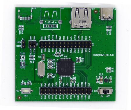
WCH CH32F203-EVT
Jump to navigation
Jump to search
This article describes specifics for the WCH CH32F203-EVT evaluation board.

Preparing for J-Link
- Connect the board with jumping wires to your J-Link (see table below)
For information about the J-Link pinout please refer to the following page: J-Link SWD pinout.
| J-Link 20 pin debug interface | Pin on evaluation board |
|---|---|
| Pin 1 (VTref) | 3V3 at P2 pin header |
| Pin 4 (GND) | GND at P2 pin header |
| Pin 7 (SWDIO) | PA14 at P2 pin header |
| Pin 9 (SWCLK) | PA13 at P2 pin header |
- Power the board via P12 (USB-C)
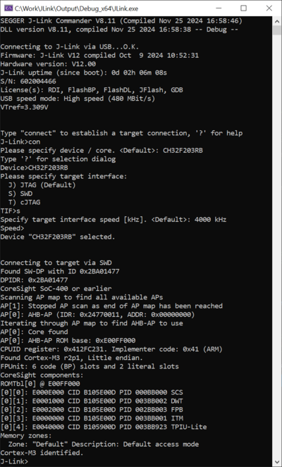
- Verify the Connection with e.g. J-Link Commander. The output should look as follows:
Example Project
The following example project was created with the SEGGER Embedded Studio project wizard and runs out-of-the-box on the WCH CH32F203-EVT.
It is a simple Hello World sample linked into the code flash.
SETUP
- J-Link software: V8.10i
- Embedded Studio: V8.18
- Hardware: WCH CH32F203-EVT
- Link: File:WCH CH32F203-EVT TestProject ES V818.zip
