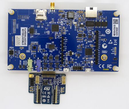
STM32H735G-DK
This article describes specifics for the ST STM32H735G-DK evaluation board.

Preparing for J-Link
- Connect the J-Link to CN7
- Power the board via CN14
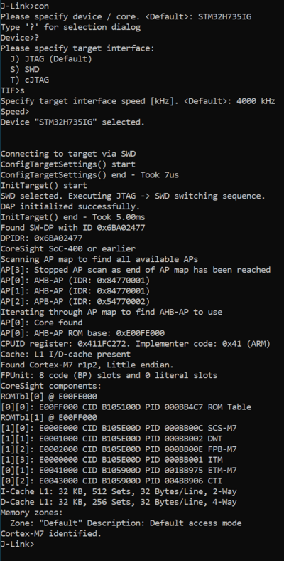
- Verify the Connection with e.g. J-Link Commander. The output should look as follows:
Example Project
The following example project was created with the SEGGER Embedded Studio project wizard and runs out-of-the-box on the ST STM32H735G-DK.
It is a simple Hello World sample linked into the internal flash.
SETUP
- Embedded Studio: V8.10b
- Hardware: ST STM32H735G-DK
- Link: File:ST STM32H735IG TestProject ES V810b.zip
QSPI Flash Programming Support
Before continuing with this article, please read the generic article about QSPI flash programming support on STM32H7 devices (STM32H7 (Q)SPI support).
In contrast to the other QSPI flash programming implementations for STM32, support has been added internally through the JLinkARM.dll and not through an open flash loader.
So in case you need another pin config, please get in contact with Segger, regarding a configurable open flash loader.
For further information how to include a open flash loader into your J-Link software, please refer to:
https://wiki.segger.com/Adding_Support_for_New_Devices#Using_a_Precompiled_Flashloader
Quad-SPI Interface Pins
The ST STM32H735-DK uses the following port pins to interface the (Octa)SPI flash.
| Alternate function | Port / Pin |
|---|---|
| OCTASPI_CLK | PF10 |
| OCTASPI_CS | PG6 |
| OCTASPI_BK0_D0 | PD11 |
| OCTASPI_BK0_D1 | PD12 |
| OCTASPI_BK0_D2 | PE2 |
| OCTASPI_BK0_D3 | PD13 |
| OCTASPI_BK1_D0 | PD4 |
| OCTASPI_BK1_D1 | PD5 |
| OCTASPI_BK1_D2 | PG9 |
| OCTASPI_BK1_D3 | PD7 |
