Renesas RA8M1
The Renesas RA8M1 are Cortex-M85 based microcontrollers.
Flash Banks
Internal Flash
| Flash Bank | Base address | Size | J-Link Support | Loaders |
|---|---|---|---|---|
| Code flash option-setting memory (secure) | 0x0300A100 | 384 B |
| |
| Code flash option-setting memory (non-secure) | 0x1300A180 | 128 B |
| |
| Data flash option-setting memory | 0x27030080 | 720 B |
| |
| Code flash (secure) | 0x02000000 | Up to 2048 KB |
| |
| Code flash (non-secure) | 0x12000000 | Up to 2048 KB |
| |
| Data flash (secure) | 0x27000000 | Up to 12 KB |
| |
| Data flash (non-secure) | 0x37000000 | Up to 12 KB |
|
QSPI Flash
QSPI flash programming requires special handling compared to internal flash. For more information about this, please see the QSPI Flash Programming Support article.
Flash programming in OSPI mode is supported for Infineon S28HL512T and S28HS512T only. Other flashes are handled in single/quad mode.
| Bank name | Base address | Maximum size | Supported pin configuration |
|---|---|---|---|
| External OSPI flash CS0 | 0x80000000 | 256 MB |
|
| External OSPI flash CS1 | 0x90000000 | 256 MB |
|
Data flash specific handling
Data flash in erased state has undefined values, therefore when using J-Flash application, "Skip blank data" and "Perform blank check" options must be disabled in project settings.
Watchdog Handling
- The device has two watchdogs: Watchdog Timer (WDT) and Independent Watchdog Timer (IWDT).
- Both watchdogs are fed during flash programming.
Device Specific Handling
Connect
During connect the current security state of the device is determined. Depending on the state J-Link will use different RAM areas for operations that require RAM (flash programming, clock speed measurements):
- OEM_PL2: 0x220D0000-0x220DFFFF
- OEM_PL1: 0x320D0000-0x320DFFFF
Reset
- The devices uses normal Cortex-M reset, no special handling necessary, like described here.
Limitations
Using OEM_PL1 state with J-Flash
Since OEM_PL1 state requires the use of non-secure RAM (0x320D0000-0x320DFFFF), the user has to ensure that the J-Flash project is set up to use this RAM area instead of the secure RAM. By default J-Flash projects are created with secure RAM area (0x220D0000-0x220DFFFF) selected.
Evaluation Boards
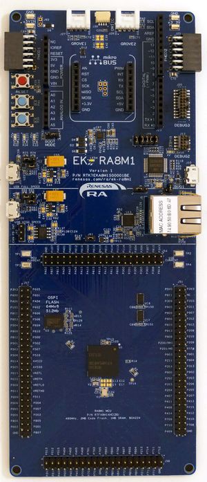
Renesas EK-RA8M1 evaluation board: http://wiki.segger.com/Renesas_EK-RA8M1
Example Application
Renesas EK-RA8M1 evaluation board: http://wiki.segger.com/Renesas_EK-RA8M1#Example_Project
Tracing on Renesas R7FA8M1
This section describes how to get started with trace on the Renesas R7FA8M1 MCUs. This section assumes that there is already a basic knowledge about trace in general (what is trace, what different implementations of trace are there, etc.). If this is not the case, we recommend to read Trace chapter in the J-Link User Manual (UM08001).
Some of the examples are shipped with a compiled .JLinkScriptfile (extension .pex), should you need the original source, please get in touch with SEGGER directly via our support system: https://www.segger.com/ticket/.
To create your own .JLinkScriptfile you can use the following guide as reference: How_to_configure_JLinkScript_files_to_enable_tracingMinimum requirements
In order to use trace on the Renesas R7FA8M1 MCU devices, the following minimum requirements have to be met:
- J-Link software version V7.98c or later
- Ozone V3.34a or later (if streaming trace and / or the sample project from below shall be used)
- J-Trace PRO version V3.0 or later for streaming trace
- J-Link Plus V12 or later for TMC/ETB trace
To rebuild the project our IDE Embedded Studio can be used. The recommended version to rebuild the projects is V8.14a. But the examples are all prebuild and work out-of-the box with Ozone, so rebuilding is not necessary.
The project below has been tested with the minimum requirements mentioned above and a EK-RA8M1.
- Example project: Renesas_RA8M1_TraceExample.zip
Streaming trace
Open the *_TracePins.jdebug project contained in the example project in Ozone.
Trace buffer (TMC/ETB)
Open the *_TraceBuffer.jdebug project contained in the example project in Ozone.
Tested Hardware
Specifics/Limitations
To enable pin tracing on this board some jumpers may need to be set. For more information about this see the board specific user manual.
Reference trace signal quality
The following pictures show oscilloscope measurements of trace signals output by the "Tested Hardware" using the example project. All measurements have been performed using a Agilent InfiniiVision DSO7034B 350 MHz 2GSa/s oscilloscope and 1156A 1.5 GHz Active Probes. If your trace signals look similar on your trace hardware, chances are good that tracing will work out-of-the-box using the example project. More information about correct trace timing can be found at the following website.
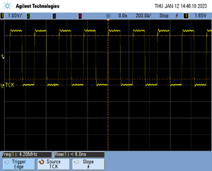
Trace clock signal quality
The trace clock signal quality shows multiple trace clock cycles on the tested hardware as reference.
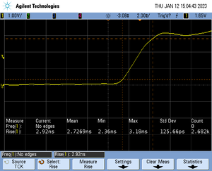
Rise time
The rise time of a signal shows the time needed for a signal to rise from logical 0 to logical 1. For this the values at 10% and 90% of the expected voltage level get used as markers. The following picture shows such a measurement for the trace clock signal.
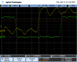
Setup time
The setup time shows the relative setup time between a trace data signal and trace clock. The measurement markers are set at 50% of the expected voltage level respectively. The following picture shows such a measurement for the trace data signal 0 relative to the trace clock signal.


