Arria 10 SoC Development Kit
Jump to navigation
Jump to search
Connecting J-Link to Altera Arria 10 SoC Development Kit
There are multiple connectors on the Altera Arria 10 board that allow J-Link connection.
| Connector | Description |
|---|---|
| J24 | Via Intel FPGA Adapter |
| J20 (FPGA TRACE) | Via J-Link Mictor 38 Adapter |
| J43 (HPS TRACE) | Via J-Link Mictor 38 Adapter |
Here is the pin config between JTAG connector(J24) on the evalboard and the J-Link debug emulator:
JTAG(J24)          J-Link
1  (TCK)     <-->  9  (TCK)
2  (ENABLEN) <-->  6  (GND)
3  (TCK)     <-->  13 (TDO)
4  (3V3)     <-->  1  (VTref)
5  (TMS)     <-->  7  (TMS)
6  (RSTn)    <-->  15 (RESET)
9  (TDI)     <-->  5  (TDI)
10 (GND)     <-->  4  (GND)
Deviating from the default settings SW3 on the needs the following setting, so only the Arria 10 device is in the JTAG chain:
SW3
1  (Arria 10)  -->  OFF (default) Arria10 JTAG Enable
2  (I/O MAX V) -->  ON  (changed) MAXV JTAG Bypass
3  (FMCA)      -->  ON  (default) FMCA JTAG Bypass
4  (FMCB)      -->  ON  (default) FMCB JTAG Bypass
5  (PCIe)      -->  ON  (default) PCIe JTAG Bypass
6  (MSTR[0])   -->  OFF (default)
7  (MSTR[1])   -->  OFF (default)
8  (MSTR[2])   -->  OFF (default)
Tracing via J43 (HPS TRACE) requires following setting :
SW3
1  (Arria 10)  -->  OFF (default) Arria10 JTAG Enable
2  (I/O MAX V) -->  ON  (changed) MAXV JTAG Bypass
3  (FMCA)      -->  ON  (default) FMCA JTAG Bypass
4  (FMCB)      -->  ON  (default) FMCB JTAG Bypass
5  (PCIe)      -->  ON  (default) PCIe JTAG Bypass
6  (MSTR[0])   -->  ON  (changed) Enable HPS TRACE
7  (MSTR[1])   -->  ON  (changed)        -"-
8  (MSTR[2])   -->  ON  (changed)        -"-
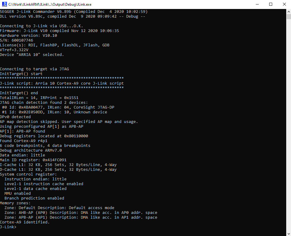
A successful connection should look like this:
