Arria 10 SoC Development Kit: Difference between revisions
Jump to navigation
Jump to search
No edit summary |
No edit summary |
||
| Line 1: | Line 1: | ||
[[Category:Evalboards]] | [[Category:Evalboards]] | ||
==Connecting J-Link to Altera Arria 10 SoC Development Kit== | ==Connecting J-Link to Altera Arria 10 SoC Development Kit== | ||
There are multiple connectors on the Altera Arria 10 board that allow J-Link connection. | |||
{| class="wikitable" | |||
!Connector | |||
!Description | |||
|- | |||
|J24 | |||
|Via [https://shop.segger.com/debug-trace-probes/debug-probes/adapters/intel-fpga-adapter Intel FPGA Adapter] | |||
|- | |||
|J20 (FPGA TRACE) | |||
|Via [https://www.segger.com/products/debug-probes/j-link/accessories/adapters/j-link-mictor-38-adapter/ J-Link Mictor 38 Adapter] | |||
|- | |||
|J43 (HPS TRACE) | |||
|Via [https://www.segger.com/products/debug-probes/j-link/accessories/adapters/j-link-mictor-38-adapter/ J-Link Mictor 38 Adapter] | |||
|} | |||
Here is the pin config between JTAG connector(J24) on the evalboard and the J-Link debug emulator: | Here is the pin config between JTAG connector(J24) on the evalboard and the J-Link debug emulator: | ||
| Line 15: | Line 30: | ||
10 (GND) <--> 4 (GND) | 10 (GND) <--> 4 (GND) | ||
Deviating from the default settings SW3 on the | Deviating from the default settings SW3 on the needs the following setting, so only the Arria 10 device is in the JTAG chain: | ||
'''SW3''' | '''SW3''' | ||
| Line 26: | Line 41: | ||
7 (MSTR[1]) --> OFF (default) | 7 (MSTR[1]) --> OFF (default) | ||
8 (MSTR[2]) --> OFF (default) | 8 (MSTR[2]) --> OFF (default) | ||
Tracing via J43 (HPS TRACE) requires following setting : | |||
'''SW3''' | |||
1 (Arria 10) --> OFF (default) Arria10 JTAG Enable | |||
2 (I/O MAX V) --> ON (changed) MAXV JTAG Bypass | |||
3 (FMCA) --> ON (default) FMCA JTAG Bypass | |||
4 (FMCB) --> ON (default) FMCB JTAG Bypass | |||
5 (PCIe) --> ON (default) PCIe JTAG Bypass | |||
6 (MSTR[0]) --> ON (changed) Enable HPS TRACE | |||
7 (MSTR[1]) --> ON (changed) -"- | |||
8 (MSTR[2]) --> ON (changed) -"- | |||
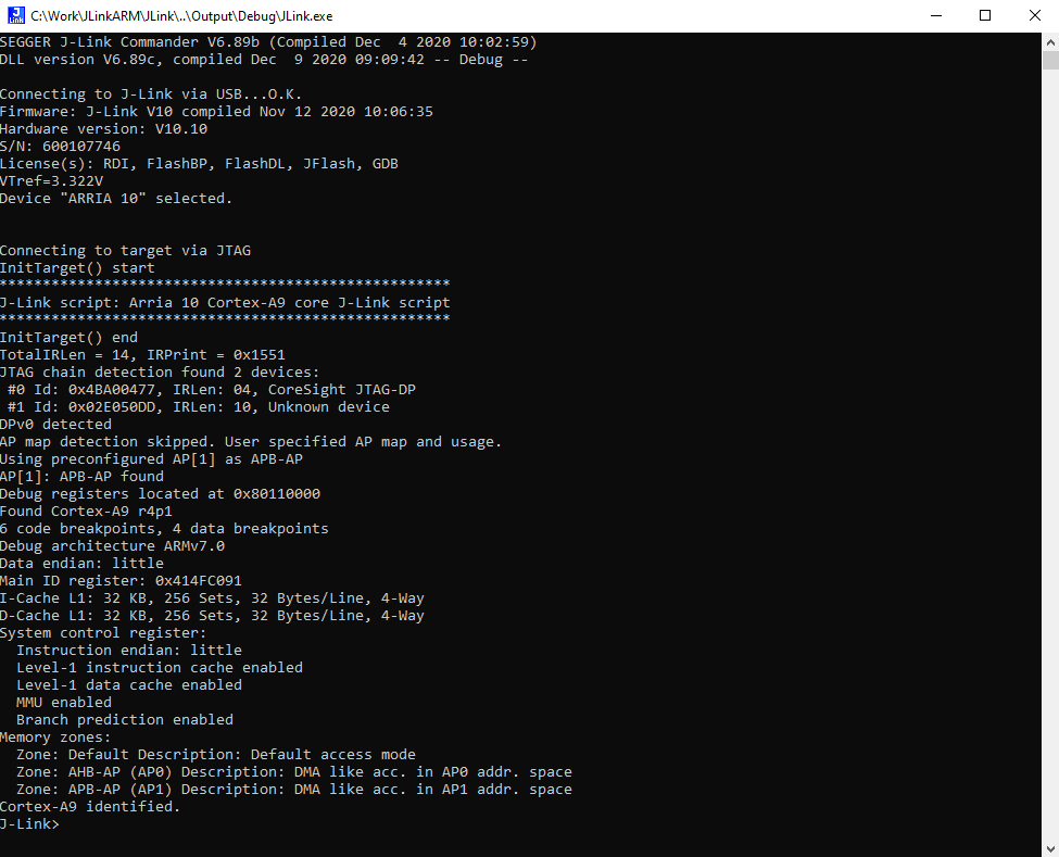
A successful connection should look like this: | A successful connection should look like this: | ||
[[File:Altera_Arria_10_J-Link.png]] | [[File:Altera_Arria_10_J-Link.png]] | ||
Revision as of 12:01, 16 October 2024
Connecting J-Link to Altera Arria 10 SoC Development Kit
There are multiple connectors on the Altera Arria 10 board that allow J-Link connection.
| Connector | Description |
|---|---|
| J24 | Via Intel FPGA Adapter |
| J20 (FPGA TRACE) | Via J-Link Mictor 38 Adapter |
| J43 (HPS TRACE) | Via J-Link Mictor 38 Adapter |
Here is the pin config between JTAG connector(J24) on the evalboard and the J-Link debug emulator:
JTAG(J24)          J-Link
1  (TCK)     <-->  9  (TCK)
2  (ENABLEN) <-->  6  (GND)
3  (TCK)     <-->  13 (TDO)
4  (3V3)     <-->  1  (VTref)
5  (TMS)     <-->  7  (TMS)
6  (RSTn)    <-->  15 (RESET)
9  (TDI)     <-->  5  (TDI)
10 (GND)     <-->  4  (GND)
Deviating from the default settings SW3 on the needs the following setting, so only the Arria 10 device is in the JTAG chain:
SW3
1  (Arria 10)  -->  OFF (default) Arria10 JTAG Enable
2  (I/O MAX V) -->  ON  (changed) MAXV JTAG Bypass
3  (FMCA)      -->  ON  (default) FMCA JTAG Bypass
4  (FMCB)      -->  ON  (default) FMCB JTAG Bypass
5  (PCIe)      -->  ON  (default) PCIe JTAG Bypass
6  (MSTR[0])   -->  OFF (default)
7  (MSTR[1])   -->  OFF (default)
8  (MSTR[2])   -->  OFF (default)
Tracing via J43 (HPS TRACE) requires following setting :
SW3
1  (Arria 10)  -->  OFF (default) Arria10 JTAG Enable
2  (I/O MAX V) -->  ON  (changed) MAXV JTAG Bypass
3  (FMCA)      -->  ON  (default) FMCA JTAG Bypass
4  (FMCB)      -->  ON  (default) FMCB JTAG Bypass
5  (PCIe)      -->  ON  (default) PCIe JTAG Bypass
6  (MSTR[0])   -->  ON  (changed) Enable HPS TRACE
7  (MSTR[1])   -->  ON  (changed)        -"-
8  (MSTR[2])   -->  ON  (changed)        -"-
A successful connection should look like this:
