Flasher - Hardware: Difference between revisions
(The chapter of UM08022 was exported to this page.) |
m (→JTAG Isolator: Updated JTAG Isolator Image) |
||
| Line 133: | Line 133: | ||
For more information about the JTAG Isolator, please refer to ''J-Link JTAG Isolator User Manual'' (UM08010) which can be downloaded from our website.<br> | For more information about the JTAG Isolator, please refer to ''J-Link JTAG Isolator User Manual'' (UM08010) which can be downloaded from our website.<br> | ||
[[File:JTAG_Isolator_Port. | [[File:JTAG_Isolator_Port.png]] | ||
=== Pinout === | === Pinout === | ||
Revision as of 13:42, 29 July 2024
This chapter gives an overview about Flasher specific hardware details, such as the pinouts and available adapters.
Flasher ARM 20-pin JTAG/SWD Connector
Flasher has a JTAG connector compatible with ARM's Multi-ICE. The JTAG connector is a 20 way Insulation Displacement Connector (IDC) keyed box header (2.54mm male) that mates with IDC sockets mounted on a ribbon cable.
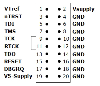
Pinout JTAG
The following table lists the Flasher JTAG pinout.
| PIN | SIGNAL | TYPE | Description |
|---|---|---|---|
| 1 | VTref | Input | This is the target reference voltage. It is used to check if the target has power, to create the logic-level reference for the input comparators and to control the output logic levels to the target. It is normally fed from Vdd of the target board and must not have a series resistor. |
| 2 | Vsupply | NC | This pin is not connected to Flasher ARM. It is reserved for compatibility with other equipment. Connect to Vdd or leave open in target system. |
| 3 | nTRST | Output | JTAG Reset. Output from Flasher ARM to the Reset signal of the target JTAG port. Typically connected to nTRST of the target CPU. This pin is normally pulled HIGH on the target to avoid unintentional resets when there is no connection. |
| 5 | TDI | Output | JTAG data input of target CPU. It is recommended that this pin is pulled to a defined state on the target board. Typically connected to TDI of target CPU. |
| 7 | TMS | Output | JTAG mode set input of target CPU. This pin should be pulled up on the target. Typically connected to TMS of target CPU. |
| 9 | TCK | Output | JTAG clock signal to target CPU. It is recommended that this pin is pulled to a defined state of the target board. Typically connected to TCK of target CPU. |
| 11 | RTCK | Input | Return test clock signal from the target. Some targets must synchronize the JTAG inputs to internal clocks. To assist in meeting this requirement, you can use a returned, and retimed, TCK to dynamically control the TCK rate. Flasher ARM supports adaptive clocking, which waits for TCK changes to be echoed correctly before making further changes. Connect to RTCK if available, otherwise to GND. |
| 13 | TDO | Input | JTAG data output from target CPU. Typically connected to TDO of target CPU. |
| 15 | RESET | I/O | Target CPU reset signal. Typically connected to the RESET pin of the target CPU, which is typically called "nRST", "nRESET" or "RESET". |
| 17 | DBGRQ | NC | This pin is not connected in Flasher ARM. It is reserved for compatibility with other equipment to be used as a debug request signal to the target system. Typically connected to DBGRQ if available, otherwise left open. |
| 19 | 5V-Target supply | Output | This pin can be used to supply power to the target board. Please note the specifications. #Target power supply |
Pins 4, 6, 8, 10, 12, 14, 16, 18, 20 are GND pins connected to GND in Flasher ARM. They should also be connected to GND in the target system.
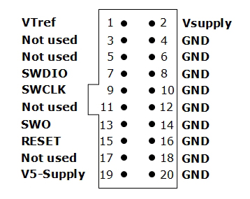
Pinout SWD
The 20-pin connector of Flasher is also compatible to ARM's Serial Wire Debug (SWD) interface.
The following table lists the J-Link / J-Trace SWD pinout.
| PIN | SIGNAL | TYPE | Description |
|---|---|---|---|
| 1 | VTref | Input | This is the target reference voltage. It is used to check if the target has power, to create the logic-level reference for the input comparators and to control the output logic levels to the target. It is normally fed from Vdd of the target board and must not have a series resistor. |
| 2 | Vsupply | NC | This pin is not connected in J-Link. It is reserved for compatibility with other equipment. Connect to Vdd or leave open in target system. |
| 3 | Not Used | NC | This pin is not used by J-Link. If the device may also be accessed via JTAG, this pin may be connected to nTRST, otherwise leave open. |
| 5 | Not used | NC | This pin is not used by J-Link. If the device may also be accessed via JTAG, this pin may be connected to TDI, otherwise leave open. |
| 7 | SWDIO | I/O | Single bi-directional data pin. |
| 9 | SWCLK | Output | Clock signal to target CPU. It is recommended that this pin is pulled to a defined state of the target board. Typically connected to TCK of target CPU. |
| 11 | Not used | NC | This pin is not used by J-Link. This pin is not used by J-Link when operating in SWD mode. If the device may also be accessed via JTAG, this pin may be connected to RTCK, otherwise leave open. |
| 13 | SWO | Output | Serial Wire Output trace port. (Optional, not required for SWD communication.) |
| 15 | RESET | I/O | Target CPU reset signal. Typically connected to the RESET pin of the target CPU, which is typically called "nRST", "nRESET" or "RESET". |
| 17 | Not used | NC | This pin is not connected in J-Link. |
| 19 | 5V-Target supply | Output | This pin can be used to supply power to the target board. Please note the specifications. #Target power supply |
Pins 4, 6, 8, 10, 12, 14, 16, 18, 20 are GND pins connected to GND in J-Link. They should also be connected to GND in the target system.
Target power supply
Pin 19 of the connector can be used to supply power to the target hardware. Supply voltage is 5V, max. current is 400mA.
The output current is monitored and protected against overload and short-circuit.
Power can be controlled via the J-Link commander. The following commands are available to control power:
| Command | Explanation |
|---|---|
| power on | Switch target power on |
| power off | Switch target power off |
| power on perm | Set target power supply default to "on" |
| power off perm | Set target power supply default to "off" |
Target board design
We strongly advise following the recommendations given by the chip manufacturer. These recommendations are normally in line with the recommendations.
Please refer to the the appropriate tables depending on the core:
In case of doubt you should follow the recommendations given by the semiconductor manufacturer.
Pull-up/pull-down resistors
Unless otherwise specified by developer's manual, pull-ups/pull-downs are recommended to be between 2.2 kOhms and 47 kOhms.
RESET, nTRST
The debug logic is reset independently from the CPU core with nTRST. For the core to operate correctly it is essential that both signals are asserted after power-up.
The advantage of having separate connection to the two reset signals is that it allows the developer performing software debug to setup breakpoints, which are retained by the debug logic even when the core is reset. (For example, at the reset vector address, to allow the code to be single-stepped as soon as it comes out of reset). This can be particularly useful when first trying to bring up a board with a new ASIC.
Adapters
JTAG Isolator
The JTAG Isolator can be connected between Flasher and JTAG adapter, to provide electrical isolation. This is essential when the development tools are not connected to the same ground as the application.
For more information about the JTAG Isolator, please refer to J-Link JTAG Isolator User Manual (UM08010) which can be downloaded from our website.
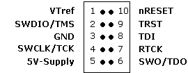
Pinout
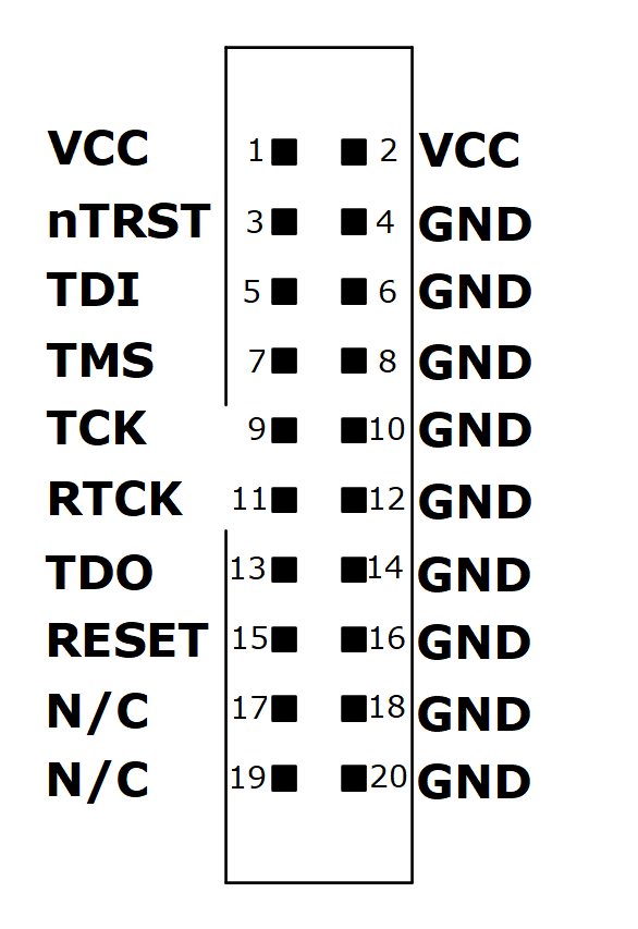
The following table shows the target-side pinout of the J-Link JTAG Isolator.
| Pin | Signal | Type | Description |
|---|---|---|---|
| 1 | VCC | Output | The target side of the isolator draws power over this pin. |
| 2 | VCC | Output | The target side of the isolator draws power over this pin. |
| 3 | nTRST | Output | JTAG Reset. Output from Flasher to the Reset signal of the target JTAG port. Typically connected to nTRST of the target CPU. This pin is normally pulled HIGH on the target to avoid unintentional resets when there is no connection. |
| 5 | TDI | Output | JTAG data input of target CPU. It is recommended that this pin is pulled to a defined state on the target board. Typically connected to TDI of target CPU. |
| 7 | TMS | Output | JTAG mode set input of target CPU. This pin should be pulled up on the target. Typically connected to TMS of target CPU. |
| 9 | TCK | Output | JTAG clock signal to target CPU. It is recommended that this pin is pulled to a defined state of the target board. Typically connected to TCK of target CPU. |
| 11 | RTCK | Input | Return test clock signal from the target. Some targets must synchronize the JTAG inputs to internal clocks. To assist in meeting this requirement, you can use a returned, and retimed, TCK to dynamically control the TCK rate. |
| 13 | TDO | Input | JTAG data output from target CPU. Typically connected to TDO of target CPU. |
| 15 | RESET | I/O | Target CPU reset signal. Typically connected to the RESET pin of the target CPU, which is typically called "nRST", "nRESET" or "RESET". |
| 17 | N/C | N/C | This pin is not connected on the target side of the isolator. |
| 19 | N/C | N/C | This pin is not connected on the target side of the isolator. |
Pins 4, 6, 8, 10, 12, 14, 16, 18, 20 are connected to GND.
Safety
This isolator provides basic isolation only. Do not use with hazardous voltages without further protection measures to avoid risk of electrical shock and fire.
SEGGER isolators provide a basic isolation to withstand high voltages as mentioned in the resp. technical data section. To preserve integrity of human beings when dealing with potential hazardous voltages it is mandatory to have a second protection measure in place in case the first insulation barrier fails. This is called double or reinforced isolation. How this double isolation can be achieved depends on the use case or application setup. Also check your the local safety related directives valid for your country to make sure all requirements are met.
J-Link Needle Adapter
To connect to the J-Link OB via programming interface the J-Link Needle Adapter is recommended.
Why to choose the J-Link Needle Adapter:
- No additional connector required on your PCB
- Very small footprint
- High reliability spring pins for secure connections
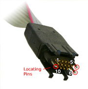
- Designed with 3 locating pins, so the adapter can not be connected the wrong way
- No external power supply required! The J-Link Needle Adapter comes with the option to power the target hardware via J-Link.
These features make the J-Link Needle Adapter the perfect solution for production purposes.
The pinout of the J-Link Needle Adapter is based on the pinout of the needle adapter by Tag-Connect.
Please note, that both pinouts are not identical since the J-Link Needle Adapter comes with a 5V-supply pin.
As you can see on the image below, the three locating pins ensure, that the adapter cannot be connected to the PCB the wrong way.
Moreover, the two "legs" on each side of the connector guarantee a stable and secure contact between pins and the PCB.
The J-Link Needle Adapter can be connected to J-Link via the 20-pin 0.1 JTAG to a 10-pin needle connector.
Target interface pin states in idle
After completing a target operation (e.g. production programming via #AUTO), Flasher configures all target interface pins to input with the following exceptions:
- Reset pin (Pin 15) By default, the reset pin remains unchanged. If the "Start application" option is enabled, the reset pin is set to high output.
- 5V-Supply (Pin 19) The state of this pin in idle depends on the configuration of the Target power supply.
If the target interface pins are configured as inputs, the target can drive the status of the pins with minimal interference from the Flasher. It is possible for minimal electrical currents to flow between Flasher and the target.
In case a complete electrical disconnection between Flasher and target is required, we recommend to make use of the SEGGER Relay Adapter.
How to determine the hardware version
To determine the hardware version of your Flasher, the first step should be to look at the label at the bottom side of the unit.
Flasher has the hardware version printed on the back label.
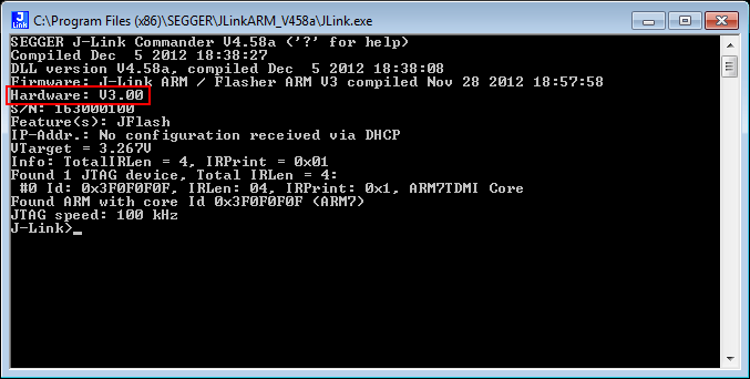
If this is not the case with your Flasher, you can use JLink.exe to determine your hardware version (if Flasher is in PC-based mode).
As part of the initial message, the hardware version is displayed. For more information about how to ensure that Flasher is in PC-based mode, please refer to PC-based mode.
