Microchip Curiosity GX1000: Difference between revisions
Jump to navigation
Jump to search
| Line 32: | Line 32: | ||
* The wiring should look as follows: | * The wiring should look as follows: | ||
[[File:Microchip_PIC64_Curiosity_Kit_V2_Wired.JPG|450px]] | [[File:Microchip_PIC64_Curiosity_Kit_V2_Wired.JPG|450px]] | ||
* Disable or remove the FTDI chip as it will interfere with the JTAG singals. | |||
** You can either desolder the chip or keep it in reset by e.g. desoldering R162 and C279 and shorting the pads of C279. | |||
*Power the board via USB-C connector. | *Power the board via USB-C connector. | ||
* Verify the Connection with e.g. [https://wiki.segger.com/J-Link_cannot_connect_to_the_CPU#Verify_functionality_using_J-Link_Commander J-Link Commander]. The output should look as follows: | * Verify the Connection with e.g. [https://wiki.segger.com/J-Link_cannot_connect_to_the_CPU#Verify_functionality_using_J-Link_Commander J-Link Commander]. The output should look as follows: | ||
[[File:Microchip_PIC64_Connect.png|400px]] | [[File:Microchip_PIC64_Connect.png|400px]] | ||
Revision as of 15:08, 4 August 2025
This article describes specifics for the Microchip PIC64GX Curiosity Kit.

Preparing for J-Link
The eval kit does not have a dedicated header to connect an external debug probe. To be able to use your J-Link with the board the following steps are necessary:
- Connect the J-Link to the board via the SEGGER Flying Wire Adapter.
- Connect the adapter to this pins/testpoints:
| Adapter Pin | Board label |
|---|---|
| VTref | 3P3V |
| GND | GND |
| TRST | TRST# |
| TDI | TDI |
| TMS/SWDIO | TMS |
| TCK/SWCLK | TCK |
| TDO/SWO | TDO |
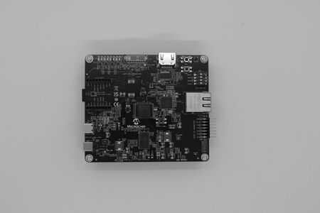
- The wiring should look as follows:
- Disable or remove the FTDI chip as it will interfere with the JTAG singals.
- You can either desolder the chip or keep it in reset by e.g. desoldering R162 and C279 and shorting the pads of C279.
- Power the board via USB-C connector.
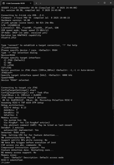
- Verify the Connection with e.g. J-Link Commander. The output should look as follows:

