NXP S32K3xx
The S32K3 family from NXP includes Cortex-M7 based MCUs in single or dual core configurations supporting ASIL B/D safety applications. The S32K3 family is supported since J-Link software version V6.89c.
Internal Flash
Supported Regions
S32K310
| Flash Bank | Base address | Size | J-Link Support |
|---|---|---|---|
| Code flash 0 | 0x00400000 | Up to 512 KB | |
| Data flash | 0x10000000 | Up to 64 KB | |
| UTEST (OTP) | 0x1B000000 | Up to 8 KB |
AB_SWAP configuration is not supported for the S32K310 yet.
S32K311
| Flash Bank | Base address | Size | J-Link Support |
|---|---|---|---|
| Code flash 0 | 0x00400000 | Up to 512 KB | |
| Code flash 1 | 0x00480000 | Up to 512 KB | |
| Data flash | 0x10000000 | Up to 64 KB | |
| UTEST (OTP) | 0x1B000000 | Up to 8 KB |
S32K312, S32K322, S32K342
| Flash Bank | Base address | Size | J-Link Support |
|---|---|---|---|
| Code flash 0 | 0x00400000 | Up to 1 MB | |
| Code flash 1 | 0x00500000 | Up to 1 MB | |
| Data flash | 0x10000000 | Up to 128 KB | |
| UTEST (OTP) | 0x1B000000 | Up to 8 KB |
S32K314, S32K324, S32K344
| Flash Bank | Base address | Size | J-Link Support |
|---|---|---|---|
| Code flash 0 | 0x00400000 | Up to 1 MB | |
| Code flash 1 | 0x00500000 | Up to 1 MB | |
| Code flash 2 | 0x00600000 | Up to 1 MB | |
| Code flash 3 | 0x00700000 | Up to 1 MB | |
| Data flash | 0x10000000 | Up to 128 KB | |
| UTEST (OTP) | 0x1B000000 | Up to 8 KB |
S32K328, S32K338, S32K348, S32K358, S32K388
| Flash Bank | Base address | Size | J-Link Support |
|---|---|---|---|
| Code flash 0 | 0x00400000 | Up to 2 MB | |
| Code flash 1 | 0x00600000 | Up to 2 MB | |
| Code flash 2 | 0x00800000 | Up to 2 MB | |
| Code flash 3 | 0x00A00000 | Up to 2 MB | |
| Data flash | 0x10000000 | Up to 128 KB | |
| UTEST (OTP) | 0x1B000000 | Up to 8 KB |
S32K341
| Flash bank | Base address | J-Link support | Flasher support | Loader | |
|---|---|---|---|---|---|
| Name | Bank size | ||||
| Code flash [1] | 0x00400000 | HSM disabled | 1 MB | ||
| HSM FULL_MEM | 1 MB | ||||
| HSM AB_SWAP | 1 MB | ||||
| Data flash [1] | 0x10000000 | HSM disabled | 128 KB | ||
| HSM FULL_MEM | 88 KB | ||||
| HSM AB_SWAP | 128 KB | ||||
| UTEST(OTP) | 0x1B000000 | N/A | 8 KB | ||
S32K364, S32K374, S32K394
| Flash Bank | Base address | Size | J-Link Support |
|---|---|---|---|
| Code flash 0 | 0x00400000 | Up to 2 MB | |
| Code flash 1 | 0x00600000 | Up to 2 MB | |
| Data flash | 0x10000000 | Up to 128 KB | |
| UTEST (OTP) | 0x1B000000 | 8 KB |
S32K356, S32K366, S32K376, S32K396
| Flash Bank | Base address | Size | J-Link Support |
|---|---|---|---|
| Code flash 0 | 0x00400000 | Up to 2 MB | |
| Code flash 1 | 0x00600000 | Up to 2 MB | |
| Code flash 2 | 0x00800000 | Up to 2 MB | |
| Data flash | 0x10000000 | Up to 128 KB | |
| UTEST (OTP) | 0x1B000000 | 8 KB |
S32K389
| Flash Bank | Base address | Size | J-Link Support |
|---|---|---|---|
| Code flash 0 | 0x00400000 | 1 MB | |
| Code flash 1 | 0x00500000 | 1 MB | |
| Code flash 2 | 0x00600000 | 2 MB | |
| Code flash 3 | 0x00800000 | 2 MB | |
| Code flash 4 | 0x00A00000 | 1 MB | |
| Code flash 5 | 0x00B00000 | 1 MB | |
| Code flash 6 | 0x00C00000 | 2 MB | |
| Code flash 7 | 0x00E00000 | 2 MB | |
| Data flash | 0x10000000 | 256 KB | |
| UTEST (OTP) | 0x1B000000 | Up to 8 KB |
ECC RAM
The ITCM and DTCM must be properly initialized with correct ECC before any read operation to avoid any code runaway or software malfucntion or core lockup. ITCM must be initialized with 64-bit writes whereas DTCM can be initialized with 32-bit or 64-bit writes. The following memory ranges are initialized by the J-Link on connect by default. Other ranges needs to be initialized by the application / boot ROM.
| Memory | Address | Size |
|---|---|---|
| ITCM0 | 0x00000000 | 32 KB |
| DTCM0 | 0x20000000 | 32 KB |
| SRAM0 | 0x20400000 | 16 KB |
Skipping DTCM0 Initialization
This script disables DTCM0 memory initialization during the connection sequence. S32K3xx_NoDTCM0Init.JLinkScript
Skipping complete RAM Initialization
This script disables the complete RAM initialization during the connection sequence. S32K3xx_NoRAMInit.JLinkScript
Initialization of the work RAM is skipped in case the attach feature of J-Link is used (exec ForceAttachTarget=1)
Watchdog Handling
- The device has up to 4 watchdogs (SWT0, SWT1, SWT2, SWT3) depending on the specific MCU and number of Cortex-M7 cores.
- If the watchdog of the core connected to is enabled, it is turned off during flash programming and turned back on afterwards.
HSE activated
In case of HSE firmware is installed, there are two configurations:
- FULL_MEM (code flash is considered as one region)
- AB_SWAP (code flash is split into two regions)
In case of FULL_MEM, the HSE is located at the end of the last code flash memory. Access to this region is prohibited.
In case of AP_SWAP is used, the code flash will be split into two regions. In this case, the HSE is available twice (once per region) and located at the end of both regions.
Multi-Core Support
Before proceeding with this article, please check out the generic article regarding Multi-Core Debugging.
The S32K3 family comes with a variety of multi-core options. Usually co-processors are disabled after reset / by default thus needs to be enabled by the J-Link on connect. Some of them are running in permanent lockstep mode, some are operating in optional lockstep mode and others are pure single core co-processors. In below, the debug related multi-core behavior of the J-Link is described for each core:
Main core (Cortex-M7_0)
Init/Setup
- Initializes the ECC RAM, see ECC RAM
- Enables debugging
- If a connection is not otherwise possible, a connect under reset is performed. See Reset
Reset
- Device specific reset is performed, see Reset
Attach
- By default, the ECC RAM is initialized thus attach is not possible. In order to attach to the target, the exec ForceAttachTarget=1 command string needs to be used.
- Attach is not possible if a connect under reset would have to be performed. See Reset
Secondary cores (Cortex-M7_1, Cortex-M7_2, Cortex-M7_3)
Init/Setup
- If the main core session has not been started / debugging is not enabled yet, the secondary core executes the enable debug sequence.
- If the secondary core is not enabled yet, it will be enabled / released from reset
- Initializes the ECC RAM, see ECC RAM
Reset
- No reset is performed.
Attach
- Attach is supported / desired. Note that the ECC RAM will be initialized anyhow. In order to skip the ECC RAM init, the exec ForceAttachTarget=1 command string needs to be used.
Reset
The J-Link performs a device specific reset sequence. The reset is executed for the main core, only. Reset of the main core, resets / disables the secondary core if used in parallel.
The reset pin needs to be connected in order to guarantee a proper reset.
Debug Authentication
The S32K3xx family supports different security mechanisms. The following table provides an overview of which types are supported and which are not:
| Silicon type | Info | J-Link Support |
|---|---|---|
| E5 | Configured for Secure boot assist flash (SBAF) | |
| E6 | Configured for secure application debug with password authentication. | |
| E7 | Configured for secure application debug with challenge/response authentication. |
Depending on the authentication level, debug access can be granted if the correct key is passed. How this is possible is described below.
Specifying the authentication code using J-Link Command String
This is the recommended method as the specified authentication key will be used for the whole session. This way, the key must not specified multiple times (e.g. if a reset is performed). The J-Link Command String needs to be passed to the J-Link DLL before establishing the target connection. The J-Link Command String SetCPUConnectIDCode <AuthKey> has to be used (see example below).
Example authentication key:
- AuthenticationKey0: 0x01234567
- AuthenticationKey1: 0x89ABCDEF
- AuthenticationKey2: 0x00224466
- AuthenticationKey3: 0x88AABBCC
exec SetCPUConnectIDCODE 67452301EFCDAB8966442200CCBBAA88
Specifying the authentication code using the ID Code dialog
If the authentication key has not been specified using the Command String although it is required to enable debug access, the following message box will pop up which allows specifying the authentication key.
Limitations
Security / Authentication
There are three different types available in regard to the security. The following table provides an overview of which types are supported and which are not:
| Silicon type | Info | J-Link Support |
|---|---|---|
| E5 | Configured for Secure boot assist flash (SBAF) | |
| E6 | Configured for secure application debug with password authentication. | |
| E7 | Configured for secure application debug with challenge/response authentication. |
SystemView
With J-Link software V7.84e ECC RAM handling was added. So it is no longer possible to run a debug session in parallel with SystemView, as the connect from SystemView will reinitialize the ECC RAM init and overwrite the RTT buffers. To avoid this the following .JLinkScript file must be added to SystemView.
S32K3xx_SystemView.JLinkScript
How to add a .JLinkScript to SystemView is explained here: J-Link_script_files#SystemView
MPU faults during connection
On some S32K3 projects, the MPU configuration restricts write access to specific memory regions. When the J-Link attempts to initialize the ITCM0 or DTCM0 RAM area during the connection sequence, these write protections can trigger an MPU fault, causing the connection to fail. To prevent this, you can add one of the following J-Link script files to your project.
Alternatively, you can modify your project’s debug configuration to avoid restricting access to the ITCM0 and DTCM0 regions.
J-Scope
Starting with J-Link software V7.84e, ECC RAM handling was introduced. Upon connect, J-Link reinitializes the RAM, which may overwrite existing RTT buffers. To prevent this behavior, one of the following .JLinkScript files can be used:
Evaluation Boards
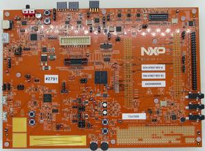
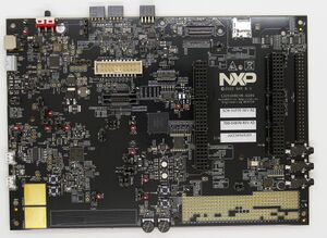
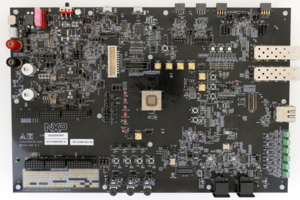
- NXP S32K3X4EVB-Q257 evaluation board: https://wiki.segger.com/NXP_S32K3X4EVB
Example Application
- NXP S32K3X4EVB evaluation board: https://wiki.segger.com/NXP_S32K3X4EVB#Example_Project
The example has been tested on the S32K3X4EVB but it should run on any S32K344 based hardware.
Tracing on NXP S32K344
Minimum requirements
In order to use trace on the NXP S32K344 MCU devices, the following minimum requirements have to be met:
- J-Link software version V8.22 or later
- Ozone V3.38d or later (if streaming trace and / or the sample project from below shall be used)
- J-Trace PRO (for Cortex-M) HW version V1.0 or later for streaming trace
To rebuild the project our IDE Embedded Studio can be used. The recommended version to rebuild the projects is V8.22. But the examples are all prebuild and work out-of-the box with Ozone, so rebuilding is not necessary.
The project below has been tested with the minimum requirements mentioned above and the following development kits.
- S32K3X4EVB-Q257: NXP_S32K344_TraceExample.zip
- S32K3X4EVB-T172: NXP_S32K344_S32K3X4EVB_TracePins.zip
Streaming trace
Open the *_TracePins.jdebug project contained in the example project in Ozone.
Trace buffer (TMC/ETB)
Open the *_TraceBuffer.jdebug project contained in the example project in Ozone.
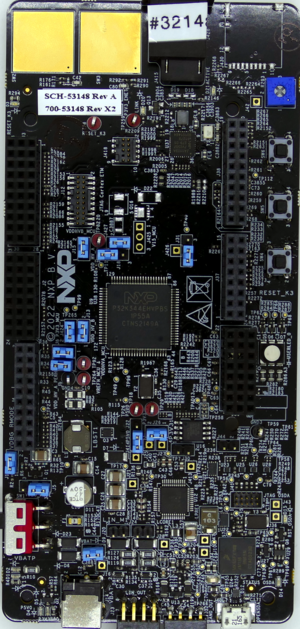
Tested Hardware
Specifics/Limitations
The S32K3X4EVB_T172 needs some solder bridges closed and resistors removed for all 4 trace data pins to work. For more information about this see the board specific schematics.
Reference trace signal quality
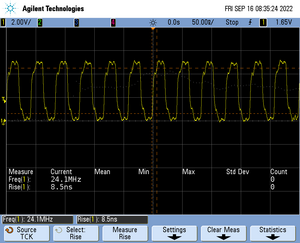
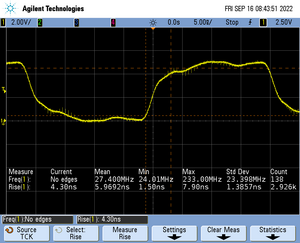
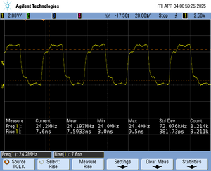
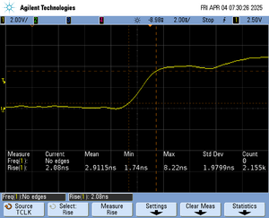
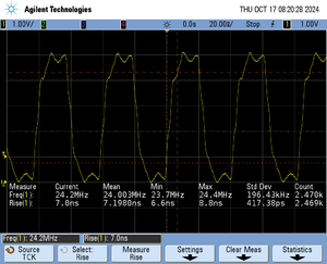
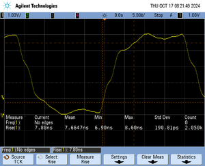
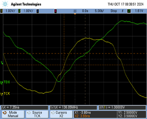
The following pictures show oscilloscope measurements of trace signals output by the NXP S32K3X4EVB-Q257 using the example project. All measurements have been performed using a Agilent InfiniiVision DSO7034B 350 MHz 2GSa/s oscilloscope and 1156A 1.5 GHz Active Probes. If your trace signals look similar on your trace hardware, chances are good that tracing will work out-of-the-box using the example project. More information about correct trace timing can be found at the following website.
Trace clock signal quality
The trace clock signal quality shows multiple trace clock cycles on the tested hardware as reference.
Rise time
The rise time of a signal shows the time needed for a signal to rise from logical 0 to logical 1. For this the values at 10% and 90% of the expected voltage level get used as markers. The following picture shows such a measurement for the trace clock signal.
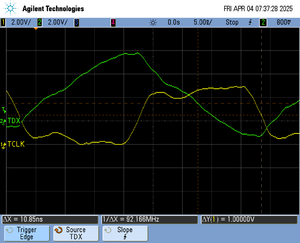
Setup time
The setup time shows the relative setup time between a trace data signal and trace clock. The measurement markers are set at 50% of the expected voltage level respectively. The following picture shows such a measurement for the trace data signal 0 relative to the trace clock signal.
Tracing on NXP S32K358
This section describes how to get started with trace on the NXP S32K358 MCUs. This section assumes that there is already a basic knowledge about trace in general (what is trace, what different implementations of trace are there, etc.). If this is not the case, we recommend to read Trace chapter in the J-Link User Manual (UM08001).
Some of the examples are shipped with a compiled .JLinkScriptfile (extension .pex), should you need the original source, please get in touch with SEGGER directly via our support system: https://www.segger.com/ticket/.
To create your own .JLinkScriptfile you can use the following guide as reference: How_to_configure_JLinkScript_files_to_enable_tracingMinimum requirements
In order to use trace on the NXP S32K358 MCU devices, the following minimum requirements have to be met:
- J-Link software version V8.24 or later
- Ozone V3.38d or later (if streaming trace and / or the sample project from below shall be used)
- J-Trace PRO version V3.0 or later for streaming trace
- J-Link Plus V12 or later for TMC/ETB trace
To rebuild the project our IDE Embedded Studio can be used. The recommended version to rebuild the projects is V8.22. But the examples are all prebuild and work out-of-the box with Ozone, so rebuilding is not necessary.
Cortex-M7_0
The project below has been tested with the minimum requirements mentioned above and a S32K3x8EVB-Q289.
- Example project: NXP_S32K358_M7_0_TraceExample.zip
Streaming trace
Open the *_TracePins.jdebug project contained in the example project in Ozone.
Trace buffer (TMC/ETB)
Open the *_TraceBuffer.jdebug project contained in the example project in Ozone.
Cortex-M7_2
The project below has been tested with the minimum requirements mentioned above and a S32K3x8EVB-Q289.
- Example project: NXP_S32K358_M7_2_TraceExample.zip
Streaming trace
Open the *_TracePins.jdebug project contained in the example project in Ozone.
Trace buffer (TMC/ETB)
Open the *_TraceBuffer.jdebug project contained in the example project in Ozone.
Tested Hardware
On this target device only the main core (Cortex-M7_0) has access to the devices peripherals in regards to the trace GPIO pins. So to be able to use pin tracing on the other cores you will need to have an application running on the main core that initializes the trace pins. Only then the example projects above for the other cores will work.
Reference trace signal quality
The following pictures show oscilloscope measurements of trace signals output by the "Tested Hardware" using the example project. All measurements have been performed using a Agilent InfiniiVision DSO7034B 350 MHz 2GSa/s oscilloscope and 1156A 1.5 GHz Active Probes. If your trace signals look similar on your trace hardware, chances are good that tracing will work out-of-the-box using the example project. More information about correct trace timing can be found at the following website.
Trace clock signal quality
The trace clock signal quality shows multiple trace clock cycles on the tested hardware as reference.
Rise time
The rise time of a signal shows the time needed for a signal to rise from logical 0 to logical 1. For this the values at 10% and 90% of the expected voltage level get used as markers. The following picture shows such a measurement for the trace clock signal.
Setup time
The setup time shows the relative setup time between a trace data signal and trace clock. The measurement markers are set at 50% of the expected voltage level respectively. The following picture shows such a measurement for the trace data signal 0 relative to the trace clock signal.
Tracing on NXP S32K388
This section describes how to get started with trace on the NXP S32K388 MCUs. This section assumes that there is already a basic knowledge about trace in general (what is trace, what different implementations of trace are there, etc.). If this is not the case, we recommend to read Trace chapter in the J-Link User Manual (UM08001).
Some of the examples are shipped with a compiled .JLinkScriptfile (extension .pex), should you need the original source, please get in touch with SEGGER directly via our support system: https://www.segger.com/ticket/.
To create your own .JLinkScriptfile you can use the following guide as reference: How_to_configure_JLinkScript_files_to_enable_tracingMinimum requirements
In order to use trace on the NXP S32K388 MCU devices, the following minimum requirements have to be met:
- J-Link software version V8.12c or later
- Ozone V3.38c or later (if streaming trace and / or the sample project from below shall be used)
- J-Trace PRO version V3.0 or later for streaming trace
- J-Link Plus V12 or later for TMC/ETB trace
To rebuild the project our IDE Embedded Studio can be used. The recommended version to rebuild the projects is V8.22. But the examples are all prebuild and work out-of-the box with Ozone, so rebuilding is not necessary.
Cortex-M7_0
The project below has been tested with the minimum requirements mentioned above and a XS32K388CVB-Q289.
- Example project: NXP_S32K388_M7_0_TraceExample.zip
Streaming trace
Open the *_TracePins.jdebug project contained in the example project in Ozone.
Trace buffer (TMC/ETB)
Open the *_TraceBuffer.jdebug project contained in the example project in Ozone.
Cortex-M7_2
The project below has been tested with the minimum requirements mentioned above and a XS32K388CVB-Q289.
- Example project: NXP_S32K388_M7_2_TraceExample.zip
Streaming trace
Open the *_TracePins.jdebug project contained in the example project in Ozone.
Trace buffer (TMC/ETB)
Open the *_TraceBuffer.jdebug project contained in the example project in Ozone.
Tested Hardware
On this target device only the main core (Cortex-M7_0) has access to the devices peripherals in regards to the trace GPIO pins. So to be able to use pin tracing on the other cores you will need to have an application running on the main core that initializes the trace pins. Only then the example projects above for the other cores will work.
Reference trace signal quality
The following pictures show oscilloscope measurements of trace signals output by the "Tested Hardware" using the example project. All measurements have been performed using a Agilent InfiniiVision DSO7034B 350 MHz 2GSa/s oscilloscope and 1156A 1.5 GHz Active Probes. If your trace signals look similar on your trace hardware, chances are good that tracing will work out-of-the-box using the example project. More information about correct trace timing can be found at the following website.
Trace clock signal quality
The trace clock signal quality shows multiple trace clock cycles on the tested hardware as reference.
Rise time
The rise time of a signal shows the time needed for a signal to rise from logical 0 to logical 1. For this the values at 10% and 90% of the expected voltage level get used as markers. The following picture shows such a measurement for the trace clock signal.
Setup time
The setup time shows the relative setup time between a trace data signal and trace clock. The measurement markers are set at 50% of the expected voltage level respectively. The following picture shows such a measurement for the trace data signal 0 relative to the trace clock signal.
Tracing on NXP S32K396
This section describes how to get started with trace on the NXP S32K396 MCUs. This section assumes that there is already a basic knowledge about trace in general (what is trace, what different implementations of trace are there, etc.). If this is not the case, we recommend to read Trace chapter in the J-Link User Manual (UM08001).
Some of the examples are shipped with a compiled .JLinkScriptfile (extension .pex), should you need the original source, please get in touch with SEGGER directly via our support system: https://www.segger.com/ticket/.
To create your own .JLinkScriptfile you can use the following guide as reference: How_to_configure_JLinkScript_files_to_enable_tracingMinimum requirements
In order to use trace on the NXP S32K396 MCU devices, the following minimum requirements have to be met:
- J-Link software version V8.24 or later
- Ozone V3.38d or later (if streaming trace and / or the sample project from below shall be used)
- J-Trace PRO version V3.0 or later for streaming trace
- J-Link Plus V12 or later for TMC/ETB trace
To rebuild the project our IDE Embedded Studio can be used. The recommended version to rebuild the projects is V8.22. But the examples are all prebuild and work out-of-the box with Ozone, so rebuilding is not necessary.
Cortex-M7_0
The project below has been tested with the minimum requirements mentioned above and a S32K396-BGA-DC1.
- Example project: NXP_S32K396_M7_0_TraceExample.zip
Streaming trace
Open the *_TracePins.jdebug project contained in the example project in Ozone.
Trace buffer (TMC/ETB)
Open the *_TraceBuffer.jdebug project contained in the example project in Ozone.
Cortex-M7_2
The project below has been tested with the minimum requirements mentioned above and a S32K396-BGA-DC1.
- Example project: NXP_S32K396_M7_2_TraceExample.zip
Streaming trace
Open the *_TracePins.jdebug project contained in the example project in Ozone.
Trace buffer (TMC/ETB)
Open the *_TraceBuffer.jdebug project contained in the example project in Ozone.
On this target device only the main core (Cortex-M7_0) has access to the devices peripherals in regards to the trace GPIO pins. So to be able to use pin tracing on the other cores you will need to have an application running on the main core that initializes the trace pins. Only then the example projects above for the other cores will work.

